Via-In-Pads Technology
- Jul 1, 2019
- 2 min read
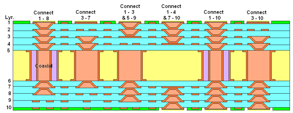
Via-In-Pads technology has been around for a few years now, but nowadays it’s becoming one of the most discussed topics amongst PCB designers and PCB fabricators. Via-in-Pads (VIP) is a technology where plated through holes are filled with conductive or non-conductive epoxy ink, subsequently planarized and plated over. Via-In-Pads are usually patterned in to BGA and uBGA pads for the direct soldering.

Growing Demand for VIP Boards
There are different schools of thought among technologists as to whether they should design the board with Via-In-Pads technologies. Few technologists strongly argue not to design boards with VIP and some strongly recommend to exploit this relatively new technology to their advantage. At Nujay Technologies we have seen a growing demand for VIP boards.
The advantages of VIP are:
· Allows miniaturization of the board
· Offers better thermal management when hole is filled with conductive material
· Makes trace routing easier specially for fine-pitch components
· Offers benefit to the High frequency designs from the shortest possible routing to bypass capacitors
· Overcomes high speed design issues and constraints i.e. low inductance
Conductive and Non-Conductive Pastes
Generally, a conductive filled via will be used when heat or a large amount of current needs to be carried from one side of the board to another. These can be found under chips that will be giving off a lot of heat where overheating is a concern. The metallic nature of the fill will naturally wick heat away from the chip to the other side of the board in many ways like a radiator.
The main drawback to conductive filled vias is the difference in CTE (Coefficient of Thermal Expansion) between the metallic fill and surrounding laminate. Metal will heat and expand much more rapidly than the surrounding laminate and this may cause fractures between the pads and the hole wall. Because of this, conductive filled vias are not recommended for Via In Pad processing where the purpose of the fill is to reinforce the stability of the copper pad that is plated over the hole.
A common misconception is that a non-conductive fill will either not pass any or only a very weak electrical signal through the via. This is not the case. The barrels of the vias will still be plated with copper the same as any other via on the board, the only difference is the empty air in barrel is replaced with the fill material. This is usually done to prevent solder or other contaminants from entering the via or provide structural support for a copper pad covering the open hole in the case of a Via In Pad. Non-Conductive fill is another term used for mask plugged vias.
PCB Cost
Via In Pad technology adds up to 10 steps to the board manufacturing process. The special requirements of via-filled material contribute to an increased cost of PCBs. However, sometimes the reduction in layer count realized by using Via In Pad technology can compensate for the added cost associated with this process.
Nujay has partnerships with domestic and off-shore PCB suppliers that offer Via-in-Pads technology. Our team is eager to get more customers on board that use Via-In-Pads Technology.


Comments