HDI PCBs
- Aug 7, 2019
- 3 min read
Updated: Sep 1, 2019
High Density Interconnect (HDI) is a method of manufacturing printed circuits with a very high density of components, typically mounted on both sides. HDI uses very small interconnecting laser drilled micro vias between individual layers and very fine traces.
By combining fine traces as small as 1 mil (25 microns), micro vias as small as 2 mils (50 microns) and multiple layers of traces and ground/power planes, the size of the traces and via circuitry percentage of the printed circuit area greatly decreases. This increases the space available to place components on both sides.

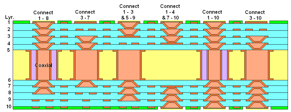
Typical application of a HDI design allows virtually any layer to connect to any adjacent layer. The HDI PCB starts with a core, in this case layers 5 and 6. It is processed as a normal double sided PCB, which provides the backbone strength for the HDI as the outer layers are quite often not glass filled and have little resistance to bending. The opposing pairs of layers of base film are laminated (layers 4 and 7), which are then laser drilled plated and filled. Normal dry film is applied and imaged, followed by copper plating and etching. Each additional pair of layers is added sequentially and final finish is applied. The extra work involved with multiple lamination cycles, multiple plating and etching cycles, as well as expensive laser time, adds up, to make HDI circuits more expensive.
To allow additional layers to connect to the underlining layer, the vias are typically filled with copper to give a solid base for connection to the top via. The laminates used to make up the HDI circuit are different than normal FR4. In many cases, the typical glass fiber based FR4 prepreg is hard to laser through, so base films of a plastic material are used. The base films allow for easier laser ablation and provide a lower CTE expansion number for the dense chip packaging used by a HDI circuit. The base films are also thinner, providing an overall thinner package. A 10 layer HDI circuit board can be as thin as 24 mils (600 mm).
Many HDI circuits are manufactured on a CIC metal core to increase the heat removal required to cool the higher density of chip packages. The metal core is also utilized to control CTE or thermal expansion. The metal core can have through via clearance holes drilled which are filled with epoxy, then re-drilled smaller and plated so as to provide an isolative sidewall but still have connectivity through the hole.

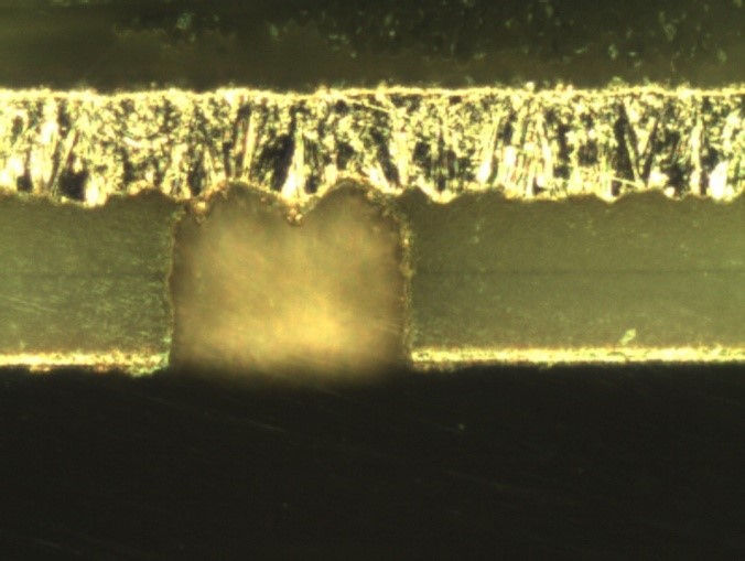
The laser drilling is a multi-step process. A thicker base copper is required on the bottom as a stop pad for the laser, so it does not cut right through. After laser ablation, the hole and base film surface is electroless plated, with a button pad so that track thickness is not increased at this stage. The button plating fills the small via level with copper, but not the copper surface of the base film. If the vias will not be stacked, the filling process will be epoxy based so that the next layer surface stays flat. After via filling the normal practices of dry film application, imaging, copper plating and etching is performed. To build more layers, a second layer set of base films is laminated on, and the process repeats itself, until all layers are finished.

Laser ablated hole; notice the thicker base copper to stop the laser
HDI circuits through their very design offer high reliability. The length of any via is short which limits the damage to the interconnect through thermal cycling. The short narrow traces and close dielectric space between layers works well with impedance balanced circuit design requirements.


Comments